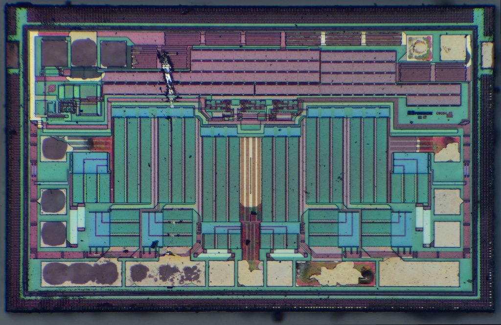
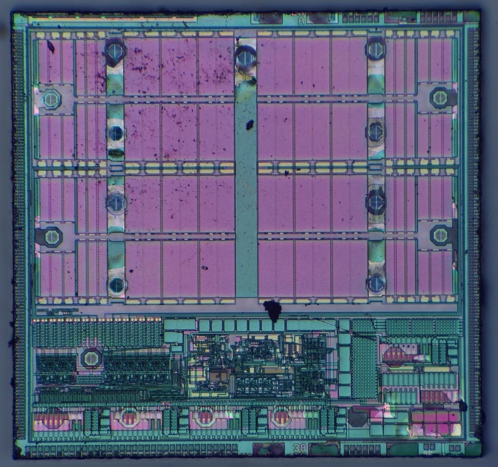
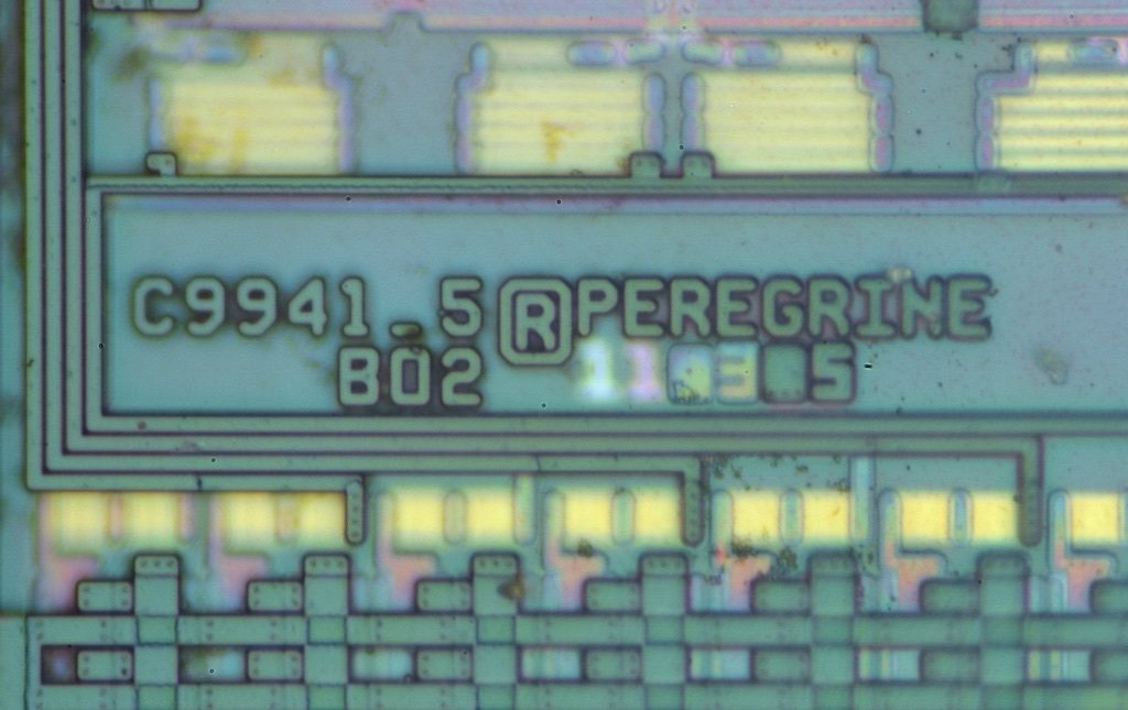
As I've gotten better at decapsulating chips, I began to find strange devices that look like little transparent cuboids with a printed circuit on one face. I don't have a macro image on hand to show this, only 2 epi-illuminated examples paired with their part codes:
- DSC_8501 copy.jpg (247.93 KiB) Viewed 1021 times

- DSC_8503 copy.jpg (122.01 KiB) Viewed 1021 times
- DSC_8502 copy.jpg (361.92 KiB) Viewed 1021 times
- DSC_8504 copy.jpg (148.47 KiB) Viewed 1021 times
Before looking up the company 'Peregrine" and finding that they specialize in Si-on-sapphire technology:
https://www.psemi.com/newsroom/blogs/15 ... n-sapphire, I wondered if the substrate was glass or quartz (since the clocks used in electronics are quartz crystal oscillators) and decided to look conoscopically, since that would tell me if there was a crystal structure or not.
Here's the conoscopic view, one of the devices is held in between the Leica 100/1.47 HCX PL APO and a Zeiss 1.3 condenser (double immersion):

- DSC_7944 copy.jpg (81.8 KiB) Viewed 1021 times
The brighter central disc occurs because the NA of the objective is larger than the NA of the condenser. Clearly, the material is a uniaxial birefringent material (so, not glass). I wondered if I could get quantitative information from this image based on the relationship between the radial coordinate 'r' on the back pupil plane and the angle of an object ray (with respect of the optical axis) 'u', r = sin(u).
Given the NA of the objective lens, I can determine the angle of the substrate crystal axis with the respect to the optical axis by measuring the distance from the center to the melatope; I calculated that angle to be 54 degrees. As it happens, the crystal structures of quartz and sapphire are the same. Checking a sapphire wafer manufactuer site, I learned that circuits are printed on the 'r-plane' (
https://melleroptics.com/primary-planes ... e-crystal/) which is oriented at 57.6 degrees from the c- axis.
Science!